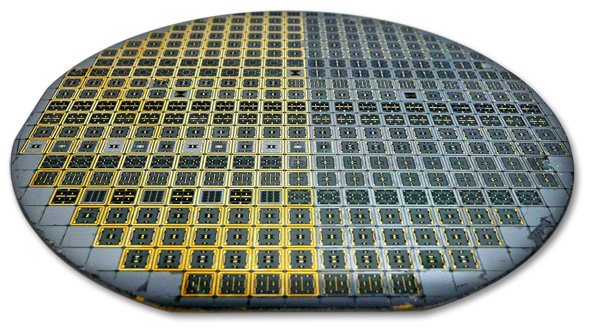
 Semiconductor wafers are the starting materials for integrated circuit manufacture. They are also referred to as substrates. The semiconductor used could either be silicon or germanium. Silicon is widely preferred since it is readily available and therefore cheaper.
SOI wafer producers in USA produce silicon wafers. The wafers are cut from a large piece of cylindrical shaped and almost perfect crystalline mass of silicon called an ingot or boule. The ingots are grown by suspending a small silicon seed crystal over molten silicon. The seed is then pulled (1m/hr) and rotated (1/2 reps) to form the ingot. The ingot is approximately 1m long and 75 to 300mm in diameter. A substance called a dopant, is always added to the molten silicon to enhance the conductivity of the produced wafers. Ingots are then sawed into wafers approximately 0.5 to 1mm thick using a diamond tipped saw. Then the surface of the wafer is then smoothened using a combination of chemical and mechanical steps. The chemical steps involve the use of an organic solvent that provides a well-wetted surface that enables uniform mass transfer during etching. This results in an optically smooth surface. Etching is a process by which parts of a wafer surface are removed. The mechanical steps involve the use of a polishing pad and a plastic retaining ring which is of a slightly bigger diameter than the wafer. The polishing head undergoes a series of rotations at various angles on the surface of the wafer. This evens out any irregular topography that might be existing on the surface of the wafer. SOI wafer producers in USA produce reliable and durable semiconductor wafers. These wafers allow top-notch fabrication and are free of flaws. Fabrication is the process by which integrated circuits are developed on the wafer surface. The smooth nature of the wafer surface allows the formation of additional circuit elements during fabrication. These wafers are tried and tested. A test is always done to ensure that the wafer has not been damaged by the processing steps. The same is done after the fabrication process. Several integrated circuits are fabricated on a single wafer. If too many integrated circuits are found faulty during testing the whole wafer is always scrapped off. Fabrication involves several steps. Photolithography is the first one and this creates images of how the circuits should look like on the wafer. Then comes Etching which removes unwanted materials from the wafer surface that is left behind after photolithography. Thermal oxidation follows. This creates a layer of silicon oxide that is protective to the wafer and acts as an isolator. Ion implantation is then done. This involves the introduction of dopant ions into the wafer. Deposition of actual materials that constitute the circuits is then done and unwanted materials are again etched away. The deposited materials are then patterned accordingly. SOI wafer producers in USA packages only those wafers that are tested and approved to be perfect. The fabricated wafers can be applied in various electronic devices for various functions. They have brought quite a big improvement in modern day electronics.
0 Comments
|
As a leading wafer supplier, WaferPro distribute Silicon wafers throughout San Jose, California, USA. WaferPro is a manufacturer of Silicon Wafers - P - Type Silicon Wafer, N - Type Silicon Wafers, FZ Wafers, SOI Wafers. Archives |
 RSS Feed
