 Variable conductivity Semiconductors in their natural state are weak conductors since a current needs the circulation of electrons, and also semiconductors have their valence bands filled up, avoiding the access circulation of new electrons. An unbalanced number of electrons will cause a current to pass throughout the product. Heterojunctions This results in an exchange of electrons and gaps in between the distinctly doped semiconducting products. The n-doped germanium will have an extra of electrons, and also the p-doped germanium will have an unwanted of gaps. The transfer takes place till balance is reached by a procedure called recombination, that causes the moving electrons from the n-type to come in contact with the moving gaps from the p-type. Excited electrons Whenever thermal balance is disrupted in a semiconducting product, the quantity of electrons and also gaps modifications. Such disturbances could happen as an outcome of a temperature level distinction or photons, that could go into the system and also produce gaps and also electrons. Light emission In specific semiconductors, excited electrons could relax by emitting light as opposed to generating warm. These semiconductors are utilized in the manufacture of light-emitting diodes and also fluorescent quantum dots. Thermal power conversion
Semiconductors have big thermoelectric power aspects making them beneficial in thermoelectric generators, in addition to high thermoelectric figures of advantage making them beneficial in thermoelectric coolers.
0 Comments
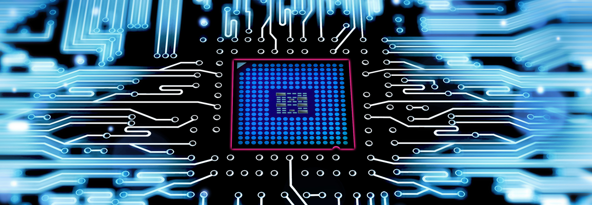
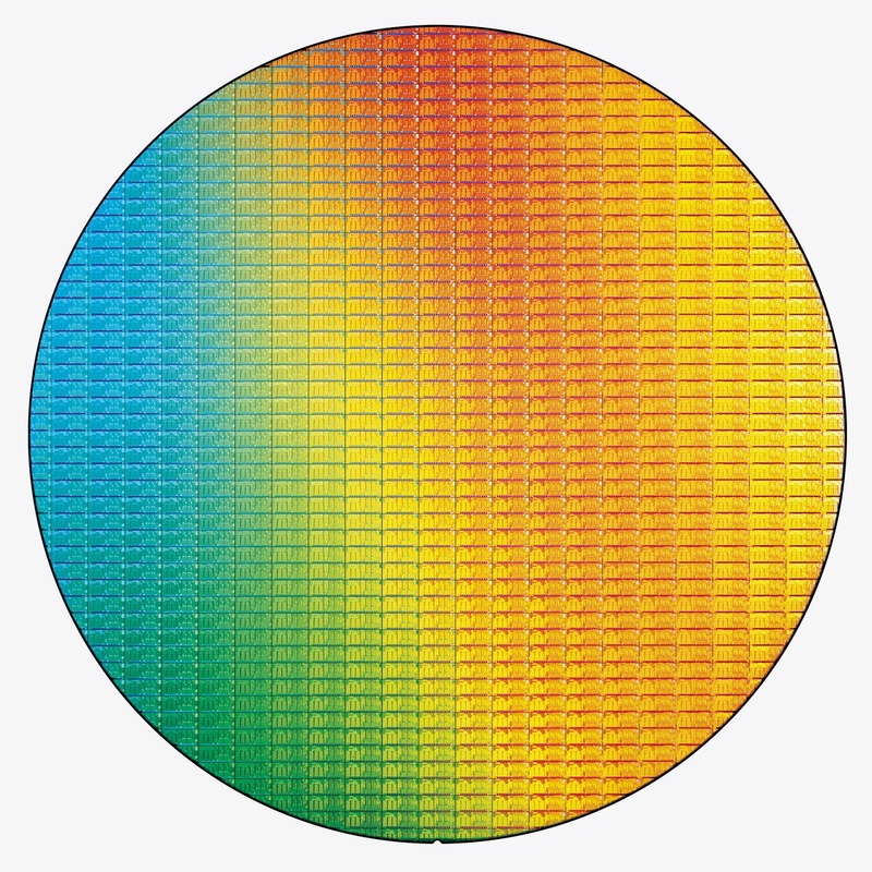
A silicon wafer is a product needed for producing semiconductors, that are discovered in all type of digital products that improve our lives. Almost all the digital accessories around us utilizes semiconductor devices. That consists of information devices like cell phones, PCs, tablet computers, and wearable computers; household devices just like TVs and a/c; and means of transportation from vehicles to trains. Currently the Internet of Things age is upon us, when everything from mobile phones to motor vehicles and commercial equipment will be Internet-connected. Need for semiconductors is taken as most likely to continue growing. Amongst the need drivers are memory and logic devices for saving and processing large quantities of information in the IoT and large information era; the different sensing units required for secure driving assistance and self-driving automobiles; and power control devices required for decreasing power usage. 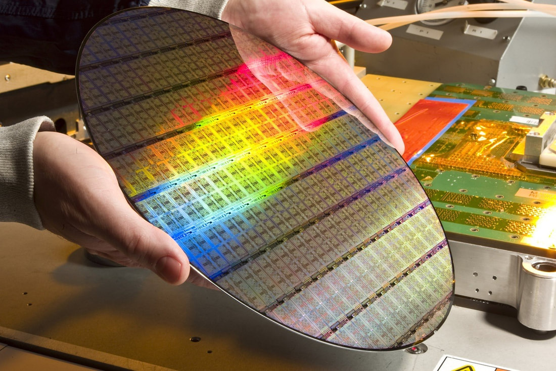 In everyday life we seldom see a silicon wafer, yet they are utilized in every kind of digital accessory and are essential in our daily lives. All type of technical invention has enabled the evolutionary advancement of digital accessories, that have added immeasurably to our daily lives and substantially helped in cultural progress. Some items have consequentially lessened, and others bigger; some lighter, some more powerful, some quicker. Engineers are continuing the fights of their predecessors, and are surpassing the accomplishments of those individuals, producing revolutionary change. For more information visit our website at www.waferpro.com
Below are 10 crucial facts you should understand about semiconductor wafers:
1. Semiconductor wafers are manufactureded from silicon that is the second-most basic element on the Globe (after oxygen) and it is the seventh-most usual element in the whole world. 2. As the sand utilized to create the semiconductor wafers needs to be a spick-and-span, much of the sand utilized for these procedures is delivered from the beaches of Australia. Not simply any kind of sand removed the beach are utilized for semiconductor wafer manufacturing. 3. Semiconductor wafers are readily available in a variety of sizes. In 1960 the 1st semiconductor wafer was made in the United States, the semiconductor wafer's sizes was 1 inch. At present the usual semiconductor wafer dimension is 1ft with foreseeable strategy to attain 1.6ft semiconductor wafers. 4. Wafers are developed with an extremely pure, basically defect-free solitary crystal product. The procedure to developing these conductors is referred to as Czochralski. Throughout this germanium, procedure or silicon is made by taking a seed crystal from a melt. Baron or phosphorus are put in the liquified inherent product in absolute amounts to dope the crystal. Soon after doping the crystal the product is after that turned in to a p-type and n-type extrinsic semiconductor. 5. Semiconductor wafers density will certainly differ considerably. Wafer density is usually found out by the mechanized strength of any product is utilized to make it. Whatever the semiconductor is created of, the wafer needs to be thick enough to sustain its current weight so it does not split throughout the handling procedure. 6. Making use of extrinsic (pure) semiconductor wafer are seen in lots of day-to-day electric products. An extrinsic semiconductor is a semiconductor which has been doped and is changed into a pure semiconductor. Applications for instance, Laser, Solar battery are based upon extrinsic semiconductor. 7. Also though silicon is taken into consideration to be the most widespread product for wafers which are utilized in electronic devices, various other substances can be utilized. III-V or II-VI products have also been utilized. Gallium arsenide or (GaAs) is a IIIV semiconductor which is manufactured throughout the Czochralski procedure. It is generally utilized as an usual wafer product. 8. Die per wafer estimation is the initial step for every engineer that desires to identify the cost of each die on a semiconductor wafer. Gross variety of dies per wafer can effortlessly and immediately determined. 9. In some certain applications the die per wafer can 1 (one) that represents that there is a solitary die on every semiconductor wafer. As the maskset reticle can't cover the whole semiconductor wafer, an unique stitches has to be done to attach the various tiles with each other. Some silicon wafer vendors have excellent experience in these sorts of applications. 10. Good storage conditions are essential to avoid contamination and/or degradation right after transport. Semiconductor Wafers which are not vacuum sealed should be put in a Nitrogen (N2) container. What are Float Zone Wafers? Float Zone wafers are the purest form of silicon slices made by the process called vertical melting zone. Vertical melting zone takes keen and smart, complicated steps, an aspect that makes the final product impurities free. Vertical melting zone leaves no room for contamination. FZ wafers are the best wafers when compared to other alternative semiconductors. Nitrogen is added to FZ semiconductor manually and in small quantities with the aim of improving its medical strength. Despite the nitrogen impurity added, FZ wafers will continue being the most sought after wafer. Therefore, the benefits and uses of FZ Wafers are many. How will you benefit with float zone wafers? Numerous benefits come with this semiconductor. First, this is a high-quality semiconductor designed from real slices of silicon. When you use this semiconductor in developing solar cells, you will experience more power conductivity than any other wafer. These wafers will absorb more heat compared to other types making them ideal for designing solar cells. When used on photo detectors, the sensitivity rate is high and hence you will receive accurate security details. Just in case you have been looking for a semiconductor that last longer; get to know that, with this FZ wafer, you are guaranteed durability. Additionally, when using these FZ wafers in leaking optical components, you will have an easier task since they are transparent and clear. This aspect makes the work of medics less complicated. The FZ wafer comes in different forms giving you the option to choose either gas or solid formulation for your purpose. 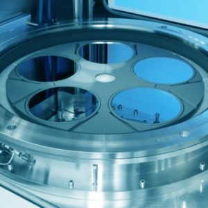 What are the uses of Float Zone Wafers?
As said earlier, this is the purest form of the silicon semiconductor and with this quality; FZ wafers have earned themselves primary uses. These include, • Making optical componentsThis is a major medical purpose that has seen FZ wafers adapted. The transparent characteristic of this semiconductor makes it easy for medics to work on people exposed to Tetra hertz radiation as they are used to manufacture lenses and windows for Tetra hertz applications. • Production of solar cells.FZ wafers have the highest solar conductivity compared to other wafers. With that in mind, this semiconductor is the best is it absorbs more heat within the same unit area With the presence of minor impurities, the rate of conductivity is incredible. • Used in photodetectors.The fact that this semiconductor is pure, it's capable of sensing electromagnetic energy making it detect anything with ease. This characteristic is the reason why FZ wafers make radio frequency chips. • Powering semiconductor devicesDue to its conductivity rate, this wafer is used in powering semiconductor devices including; Thyristors, power transistors, and rectifiers. • Manufacturing of power devices like electronic chips. • FZ wafers are used when the capacity towards resistance is needed to increase the performance of a conductor. • Used in MOS powerThis wafer is designed to handle significant power levels making your gadgets safe. To conclude, the FZ wafer has the best quality, and it's recommended for all your power devices and medical use. Having it is the best option. 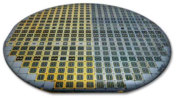 Semiconductor wafers are the starting materials for integrated circuit manufacture. They are also referred to as substrates. The semiconductor used could either be silicon or germanium. Silicon is widely preferred since it is readily available and therefore cheaper.
SOI wafer producers in USA produce silicon wafers. The wafers are cut from a large piece of cylindrical shaped and almost perfect crystalline mass of silicon called an ingot or boule. The ingots are grown by suspending a small silicon seed crystal over molten silicon. The seed is then pulled (1m/hr) and rotated (1/2 reps) to form the ingot. The ingot is approximately 1m long and 75 to 300mm in diameter. A substance called a dopant, is always added to the molten silicon to enhance the conductivity of the produced wafers. Ingots are then sawed into wafers approximately 0.5 to 1mm thick using a diamond tipped saw. Then the surface of the wafer is then smoothened using a combination of chemical and mechanical steps. The chemical steps involve the use of an organic solvent that provides a well-wetted surface that enables uniform mass transfer during etching. This results in an optically smooth surface. Etching is a process by which parts of a wafer surface are removed. The mechanical steps involve the use of a polishing pad and a plastic retaining ring which is of a slightly bigger diameter than the wafer. The polishing head undergoes a series of rotations at various angles on the surface of the wafer. This evens out any irregular topography that might be existing on the surface of the wafer. SOI wafer producers in USA produce reliable and durable semiconductor wafers. These wafers allow top-notch fabrication and are free of flaws. Fabrication is the process by which integrated circuits are developed on the wafer surface. The smooth nature of the wafer surface allows the formation of additional circuit elements during fabrication. These wafers are tried and tested. A test is always done to ensure that the wafer has not been damaged by the processing steps. The same is done after the fabrication process. Several integrated circuits are fabricated on a single wafer. If too many integrated circuits are found faulty during testing the whole wafer is always scrapped off. Fabrication involves several steps. Photolithography is the first one and this creates images of how the circuits should look like on the wafer. Then comes Etching which removes unwanted materials from the wafer surface that is left behind after photolithography. Thermal oxidation follows. This creates a layer of silicon oxide that is protective to the wafer and acts as an isolator. Ion implantation is then done. This involves the introduction of dopant ions into the wafer. Deposition of actual materials that constitute the circuits is then done and unwanted materials are again etched away. The deposited materials are then patterned accordingly. SOI wafer producers in USA packages only those wafers that are tested and approved to be perfect. The fabricated wafers can be applied in various electronic devices for various functions. They have brought quite a big improvement in modern day electronics. |
As a leading wafer supplier, WaferPro distribute Silicon wafers throughout San Jose, California, USA. WaferPro is a manufacturer of Silicon Wafers - P - Type Silicon Wafer, N - Type Silicon Wafers, FZ Wafers, SOI Wafers. Archives |
 RSS Feed
