Below are 10 crucial facts you should understand about semiconductor wafers:
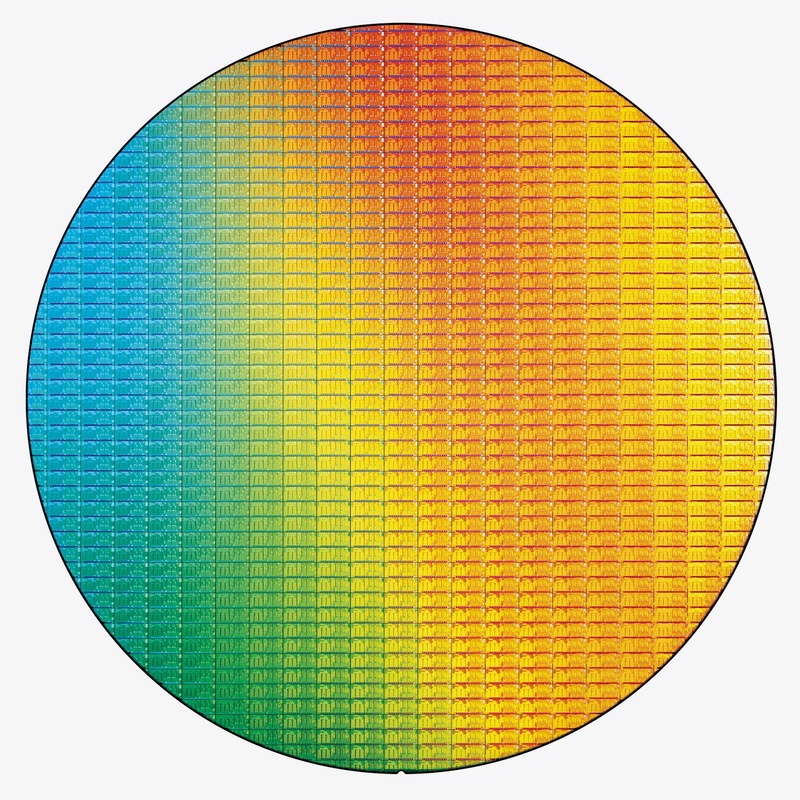
1. Semiconductor wafers are manufactureded from silicon that is the second-most basic element on the Globe (after oxygen) and it is the seventh-most usual element in the whole world. 2. As the sand utilized to create the semiconductor wafers needs to be a spick-and-span, much of the sand utilized for these procedures is delivered from the beaches of Australia. Not simply any kind of sand removed the beach are utilized for semiconductor wafer manufacturing. 3. Semiconductor wafers are readily available in a variety of sizes. In 1960 the 1st semiconductor wafer was made in the United States, the semiconductor wafer's sizes was 1 inch. At present the usual semiconductor wafer dimension is 1ft with foreseeable strategy to attain 1.6ft semiconductor wafers. 4. Wafers are developed with an extremely pure, basically defect-free solitary crystal product. The procedure to developing these conductors is referred to as Czochralski. Throughout this germanium, procedure or silicon is made by taking a seed crystal from a melt. Baron or phosphorus are put in the liquified inherent product in absolute amounts to dope the crystal. Soon after doping the crystal the product is after that turned in to a p-type and n-type extrinsic semiconductor. 5. Semiconductor wafers density will certainly differ considerably. Wafer density is usually found out by the mechanized strength of any product is utilized to make it. Whatever the semiconductor is created of, the wafer needs to be thick enough to sustain its current weight so it does not split throughout the handling procedure. 6. Making use of extrinsic (pure) semiconductor wafer are seen in lots of day-to-day electric products. An extrinsic semiconductor is a semiconductor which has been doped and is changed into a pure semiconductor. Applications for instance, Laser, Solar battery are based upon extrinsic semiconductor. 7. Also though silicon is taken into consideration to be the most widespread product for wafers which are utilized in electronic devices, various other substances can be utilized. III-V or II-VI products have also been utilized. Gallium arsenide or (GaAs) is a IIIV semiconductor which is manufactured throughout the Czochralski procedure. It is generally utilized as an usual wafer product. 8. Die per wafer estimation is the initial step for every engineer that desires to identify the cost of each die on a semiconductor wafer. Gross variety of dies per wafer can effortlessly and immediately determined. 9. In some certain applications the die per wafer can 1 (one) that represents that there is a solitary die on every semiconductor wafer. As the maskset reticle can't cover the whole semiconductor wafer, an unique stitches has to be done to attach the various tiles with each other. Some silicon wafer vendors have excellent experience in these sorts of applications. 10. Good storage conditions are essential to avoid contamination and/or degradation right after transport. Semiconductor Wafers which are not vacuum sealed should be put in a Nitrogen (N2) container.
0 Comments
Leave a Reply. |
As a leading wafer supplier, WaferPro distribute Silicon wafers throughout San Jose, California, USA. WaferPro is a manufacturer of Silicon Wafers - P - Type Silicon Wafer, N - Type Silicon Wafers, FZ Wafers, SOI Wafers. Archives |
 RSS Feed
